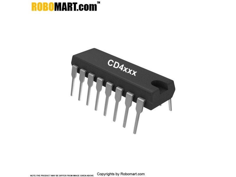
CD4502 Strobed Hex Inverter Buffer

CD4502 Strobed Hex Inverter Buffer
Availability: In stock
Brand: Generic
SKU: RM001684
₹ 59.00
Warehouse Code: R00006-S04-P03-Z01
The CD4502B consists of six inverter/buffers with 3-state outputs. A logic "1" on the OUTPUT DISABLE input produces a high-impedance state in all six outputs. This feature permits common busing of the outputs, thus simplifying system design. A Logic "1" on the INHIBIT input switches all six outputs to logic "0" if the OUTPUT DISABLE input is a logic "0". This device is capable of driving two standard TTL loads, which is equivalent to six times the JEDEC "B"-series IOL standard.
Features of CD4502 Strobed Hex Inverter Buffer:
- 2 TTL-load output drive capability.
- 3-state outputs.
- Common output-disable control.
- Inhibit control.
- 100% tested for quiescent current at 20 V.
- 5-V, 10-V, and 15-V parametric ratings.
- Maximum input current of 1 µA at 18 V over full package-temperature range; 100 nA at 18 V and 25°C.
- Meets all requirements of JEDEC Tentative Standard No. 13B, "Standard Specifications for Description of 'B' Series CMOS Devices".
Applications of CD4502 Strobed Hex Inverter Buffer:
- 3-state hex inverter for interfacing IC's with data buses.
- COS/MOS to TTL hex buffer.
Also Searched as : CD4502 IC.
*Note: Product may be differ as per shown in image
SKU: RM001637
The CD4043B IC's are quad cross-coupled 3-state CMOS NOR latches and the CD4044B types are quad cross-coupled 3-state CMOS NAND latches. Each latch ha..
₹ 39.00
SKU: RM001641
The CD4050UB devices are inverting and non-inverting hex buffers, respectively, and feature logic-level conversion using only one supply voltage (VCC)..
₹ 39.00
SKU: RM001659
The CD4069UB types consist of six CMOS inverter circuits. These devices are intended for all general-purpose inverter applications where the medium-po..
₹ 19.00
SKU: RM001685
The CD4502B consists of six inverter/buffers with 3-state outputs. A logic "1" on the OUTPUT DISABLE input produces a high-impedance state in all six ..
₹ 49.00
SKU: RM001686
The CD4504B hex voltage level-shifter consists of six circuits which shift input signals from the VCC logic level to the VDD logic level. To shift TTL..
₹ 49.00


