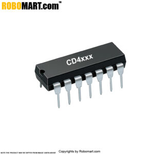
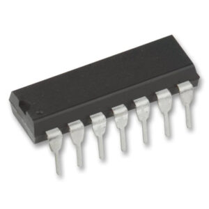
The CD4502B consists of six inverter/buffers with 3-state outputs. A logic "1" on the OUTPUT DISABLE input produces a high-impedance state in all six outputs. This feature permits common busing of the outputs, thus simplifying system design. A Logic "1" on the INHIBIT input switches all six outputs to logic "0" if the OUTPUT DISABLE input is a logic "0". This device is capable of driving two standard TTL loads, which is equivalent to six times the JEDEC "B"-series IOL standard.
Features of CD4502 Strobed Hex Inverter Buffer:
- 2 TTL-load output drive capability.
- 3-state outputs.
- Common output-disable control.
- Inhibit control.
- 100% tested for quiescent current at 20 V.
- 5-V, 10-V, and 15-V parametric ratings.
- Maximum input current of 1 ?A at 18 V over full package-temperature range; 100 nA at 18 V and 25?C.
- Meets all requirements of JEDEC Tentative Standard No. 13B, "Standard Specifications for Description of ‘B’ Series CMOS Devices".
Applications of CD4502 Strobed Hex Inverter Buffer:
- 3-state hex inverter for interfacing IC’s with data buses.
- COS/MOS to TTL hex buffer.
Also Searched as : CD4502 IC.


