CD4027B is a single monolithic chip integrated circuit containing two identical complementary-symmetry J-K flip flops. Each flip-flop has provisions for individual J, K, Set, Reset, and Clock input signals. Buffered Q and Q signals are provided as outputs. This input output arrangement provides for compatible operation with the RCA-CD4013B dual D-type flip-flop.
The CD4027B is useful in performing control, register, and toggle functions. Logic levels present at the J and K inputs along with internal self-steering control the state of each flip-flop; changes in the flip-flop state are synchronous with the postitive-going transition of the clock pulse. Set and reset functions are independent of the clock and are initiated when a high level signal is present at either the Set or Reset input.
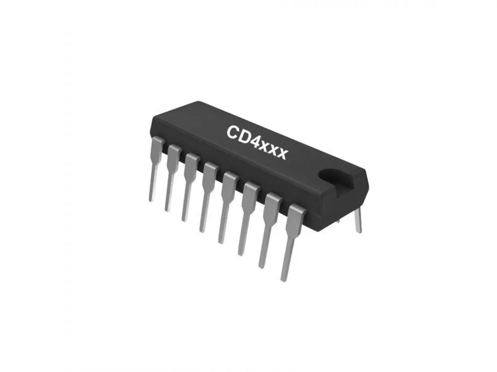
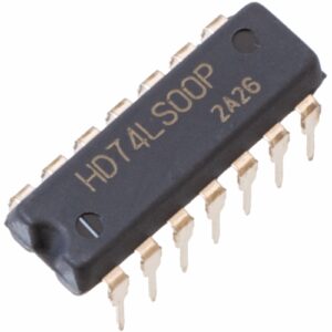
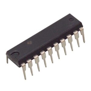
The CD4027B types are supplied in 16-lead hermetic dual-in-line ceramic packages (F3A suffix), 16-lead dual-in-line plastic packages (E suffice), 16-lead small-outline packages (M, M96, MT, and NSR suffixes), and 16-lead thin shrink small-outline packages (PW and PWR suffixes).
Features:
- Set-reset capability
- Static flip-flop operation ? retains state indefinitely with clock level either high or low
- Medium speed operation ? 16 MHz (typical) clock toggle rate at 10 V
- Standardized symmetrical output characteristics
- 100% tested for quiescent current at 20 V
- Maximum input current of 1 ?A at 18 V over full package-temperature range; 100 nA at 18 V and 25?C
- 5 V, 10 V, and 15 V parametric ratings
- Meets all requirements of JEDEC tentative standard No. 138, standard specifications for description of ‘B’ series CMOS devices
Noise margin (over full package-temperature range):
- 1 V at VDD = 5 V
- 2 V at VDD = 10 V
- 2.5 V at VDD = 15 V


