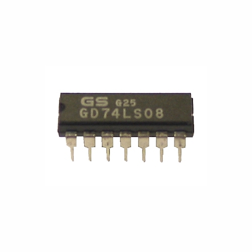
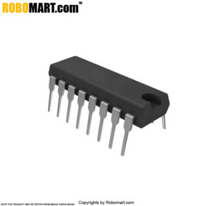
The 74ls08 quad 2 input and gates contains four independent gates each of which performs the logic AND function. 74ls08 quad 2 input and gate IC can be soldered directly to the circuit board or can be mounted on a 14 pin IC base. The 74ls08 quad 2 input and gates circuit is designed such that the AND operation of the input pins 1 & 2, 4&5, 9&10, 12,13 are produced on the pin 3 , 6, 8 & 11 respectively. Operating supply voltages to the IC can vary between 4.75V to 5V and to a maximum of 5.25V and the input logic levels to the device in ?0?(LOW) state is max. 0.8V and for ?1?(HIGH) state is min 2V.
Features of 74LS08 Quad 2-Input AND Gate:
- Operating Voltage Range 4.75V to 5V up to a maximum of 5.25V.
- Operating Temperature range : 0?C to +70?C.
- VH (Output High): 2.7V to 3.4V.
- VL (Output Low): 0.36V to 0.5V.
- Power Consumption: 4.8mA to 8.8mA.
- Operating Speed (Mhz):125 ? 250.
Applications of 74LS08 Quad 2-Input AND Gate:
- Logical Decision making.
- Circuits involving conditional operations.
- DIY projects for various logic gates based applications
