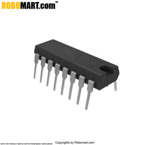
The CD40109B contains four low-to-high-voltage level-shifting circuits. Each circuit will shift a low-voltage digital-logic input signal (A, B, C, D) with logical 1 = VCC and logical 0 = VSS to a higher-voltage output signal (E, F, G, H) with logical 1 = VDD and logical 0 = VSS.
Features of CD40109 Low-To-High Voltage Level Shifter:
- Independence of power supply sequence considerations – VCC can exceed VDD, input signals can exceed both VCC and VDD.
- Up and down level-shifting capability.
- Three-state outputs with separate enable controls.
- Standardized, symmetrical output characteristics.
- 100% tested for quiescent current at 20 V.
- Maximum input current of 1 uA at 18 V over full package-temperature range; 100 nA at 18 V and 25?C.
Applications of CD40109 Low-To-High Voltage Level Shifter:
- High-or-low level-shifting with three-state outputs for unidirectional or bidirectional bussing.
- Isolation of logic subsystems using separate power supplies from supply sequencing, supply loss and supply regulation considerations.
Also Searched as : CD40109 IC.


